VHDL Structural Models for the Implementation of
Path Sensitization Test Generation
Fatemeh Khaani* and Zainalabedin Navabi
Electrical and Computer Engineering Department
Faculty of Engineering, Campus No. 2
University of Tehran
14399, Tehran IRAN
Sharif University of Technology, Tehran
Tel: +98-21-800-8485; Fax: +98-21-688690
Email: navabi_z@irearn.bitnet
Abstract
We have developed a modeling strategy in VHDL for gate level components for automatic test generation. A gate level structural description using these models is capable of generating its own test vectors for induced faults on its lines. A testbench places a fault on a line of the gate level description, and the models communicate through their ports for finding a test vector detecting the fault. This paper describes a test environment, our VHDL models, and a fault activation testbench.
1. Introduction
In the area of digital system design, test generation plays an important role. The process of finding input test vectors for detecting possible circuit faults is referred to as test generation. Fault oriented deterministic test generation is referred to the algorithmic generation of a test vector that targets a specific fault in the circuit. The D-algorithm and PODEM are such test generation methods. These algorithms are generally slow and limited in scope. A uniform test environment in which various test related tools such as test generation and fault reduction programs are interactively used, can make up for the inefficiency of test generation programs.
Because VHDL has become an important part of the design automation of digital systems, it is appropriate to think of this language as a tool that can be used in all aspects of digital design. Ideally, the same language and circuit description used for design and simulation should be used for the generation of test vectors and fault dictionaries. Using VHDL for test generation is an important step towards using VHDL as the basis of an integrated design environment for digital circuits. Furthermore, the use of concurrent programming techniques, such as those available in VHDL, can benefit test related programs for their implementation on distributed systems.
We have developed VHDL models for test generation. The models generate test using a sensitized path, deterministic fault oriented test generation method. Basic logical gate models and line resolution functions constitute the main part of our modeling. For test generation, a testbench uses a structural description of hardware bound to our test generation gate models, and activates a fault on a resolved circuit line. The models interact through their ports and find a test vector for the fault. This test vector will be reported by the testbench.
During the generation of test, the models are placed in two main modes of propagation and justification. In the propagation mode, the models interact through their ports for finding a sensitized path from the site of an introduced fault to the primary outputs. In the justification mode, the models justify node values by justifying a set of values on the primary inputs. The values found on the primary inputs constitute the test vector for the introduced fault.
This paper discusses a general test environment, VHDL based path sensitization test generation, VHDL models for test generation and details of our VHDL test generation methodology. Section 2 discusses test in VHDL and presents a justification for the use of VHDL in such environments. In Section 3 we will present an overall view of the VHDL test generation models. Details of the models and VHDL coding techniques will be discussed in Section 4. Although many test environments can take advantage of VHDL test generation models, a simplified testbench for the activation and usage of our models will be demonstrated in Section 5. In conclusions, Section 6, a simple circuit and test vectors generated for this example will be presented.
2. VHDL In Test Generation
A general design environment consists of various CAD tools for simulation, synthesis and test. In an ideal situation all such tools work in an integrated environment using the same file formats and platforms.
2.1. A Design Environment
A typical automated design, shown in Figure 1, begins with a high level description of the design. After high level design verification, the design is synthesized into a gate list which can be used as the input of a low level simulation as well as a test generation program. Generation of fault dictionaries and fault lists are also done at this stage using the same netlist. After test generation, and design verification, the netlist is used as input to a placement and wiring program for the final hardware generation and fabrication.
Present CAD tools based on VHDL make this language an ideal basis for the development of an integrated design automation environment. Although extensive works has been done on VHDL based simulation and synthesis, test generation and other test related issues are still to explore the capabilities of VHDL.
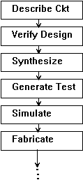
Figure 1. A typical automated design environment
2.2. Why VHDL?
An initial requirement in the design of VHDL was to be able to have a media for design documentation, synthesis, simulation and test of digital systems. Although simulation and synthesis have been successful in using this language, little attention has been given to test and test applications with VHDL. Using VHDL in test will enable a designer to simulate, design and test various parts of his circuit under the same environment. Thus using VHDL for test generation is an important step in taking advantage of this standard in test applications.
Strong support for the libraries makes VHDL an appropriate tool for use in an integrated design environment. A VHDL netlist can be used for simulation by binding its components to a simulation library. The same netlist can be bound to a test generation library for test generation for the circuit.
The syntax and semantics of VHDL make the implementation of various test related problems possible in this language. Concurrency in the language, resolution functions, and event driven nature of the language are useful in the implementation of test generation.
In addition to test generation, we have used VHDL for critical path analysis, fault simulation, and fault collapsing. The set of these test related tools, and using them along with present synthesis and simulation programs, can create an integrated design environment based on VHDL. In this environment, use of various test programs can be intelligently decided by a VHDL test program. Appropriate use of fault lists, using fault list generation programs, choosing fault-independent test generation versus fault-based test generation are tasks that an overall VHDL program can make decisions on.
3. Model Abstraction
In our method of test generation in VHDL, we start with a VHDL netlist of a combinational circuit. The components of this netlist are basic logical gates, and test is generated by special test models that we have developed for these gates. In implementing the VHDL gate models, we have used the path sensitization method and D notation for generating tests for SSFs using structural model of the given circuit. In this section we will describe the general strategies used in the development of VHDL models for structural test generation. The next section describes details of the models.
3.1. Gate Level Modeling
As mentioned above, the focus of our modeling is for the structural test generation. This implies that the analysis is based on a structural, rather than a functional, model of the circuit. The components of this structural model are primitive logical gates; AND, OR, NAND, NOR and NOT.
In addition, for resolving problems associated with reconvergent fanouts, a fanout component has also been used. Using components for fanout is a common approach in fault simulation and test generation [3]. A fanout component has one input and two outputs. Any number of these components can be cascaded together for obtaining multi-output fanouts.
3.2. Bidirectionality
Sensitized path method generates test in two phases, fault propagation and line justification. Thus it is clear that a gate must be able to react to changes on its inputs as well as its output (or outputs in the case of fanout components). In propagating values towards primary outputs, gates take input values and generate output values, and in justifying a set of values at the primary outputs, gates propagate values from their output to their inputs and towards the primary inputs.
To make this bi-directional behavior possible, INOUT has been used for the mode of all ports. When in the propagation mode, gates only react to events on their inputs, and when in the justification mode, gates react to transactions on their outputs as well as on their inputs. Another mode of operation is initialization, in which gates are sensitive to events on both their inputs and outputs.
3.3. Node Resolutions
Since all lines are INOUT, each interconnecting line is driven by at least two drivers. Therefore, we have used resolved signals for all interconnecting lines. This enables gates to use their ports in both directions for fault propagation and line justification.
Using resolved signals allows the corresponding resolution function to resolve conflicts that occur between a gate output and a gate input. When a conflict occurs, the resolution function informs both conflicting gates. Such gates will take appropriate actions according to the type of the conflict.
The next section presents a more detailed view of the behavior of the models and the resolution functions.
4. Modeling Details
We have used VHDL for the implementation of path sensitization test generation methodology. For this purpose a test generation model is developed for gate level hardware primitives. For test generation of a logical circuit, circuit primitives are bound to test models, and by proper fault insertion and gate activation, a test is generated for that specific fault. In this section we will describe the details of the models for path sensitization test generation.
4.1. How Models Work
Each gate model is designed to be able 1) to receive a fault at one of its inputs and propagate the fault to its output, and 2) to receive a signal on its output and justify its inputs accordingly.
Fault representation is done by the use of the D notation. In this notation D and DBAR values represent faulty node values. D (DBAR) at a node indicates that the good circuit value at this node is '1' ('0') and the faulty value is '0' ('1'). Figure 2 shows a minimum logic value system for the implementation of test generation in VHDL.
'0' : A line value of '0'
'1' : A line value of '1'
'X' : either a '0' or a '1'
D : A faulty line value, Good '1' & Bad '0' (1/0)
DBAR : A faulty line value, Good '0' & Bad '1' (0/1)
'U': Undefined value ( initial value of all nodes)
Figure 2. Minimum logic value system
4.1.1. Fault Propagation
Initially, for fault activation, a D or DBAR value is placed on a circuit node. The model sensing this event (a delta time later) propagates this value to its output node. The gates seeing this propagated value (at the next delta time values) at their inputs continue the propagation process until the error (D or DBAR) reaches a primary output several delta times later than the original placement of fault. At this point the justification process must begin.
4.1.2. Justification
In the justification process events originate on the gate outputs, and each gate model places values on its unassigned inputs such that these values justify its output value. In order for the gates to be able to distinguish between propagation and justification phases of operation, we have separated these two phases by 1femtosecond. As shown in the illustration of Figure 3, at a certain time ti an event on a node causes all gates to propagate input value(s) to their outputs. At this same time, a primary output receives the error. At time ti+1femtosecond the error value (D or DBAR) at the primary outputs are placed back on these lines. Gates sensing these transactions begin operating in the justification mode. Each gate depending on its output value and its inputs that were valued in the propagation phase, determines certain values for its undecided inputs. Assignment of these values to the inputs causes the justification process to go farther towards the primary inputs. When the primary inputs are justified, the test for the fault applied at time ti has been found.
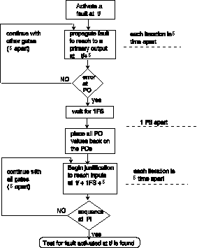
Figure 3. Propagation and justification phases
4.1.3. Preparation For Next Fault
Before applying the next fault, the circuit is reset (initialized) at time ti+2 femtoseconds. In this phase SU value (Strong 'U') will be imposed on all circuit nodes. An SU value overrides all previous node values.
The next fault is applied after the circuit node values are reset. At time ti+1 a new fault will be placed on a circuit node and the processes of propagation and justification begin for this fault. The difference between ti+1 and ti has chosen to be at least 3 femtoseconds. Figure 4 shows timing of these phases of operation.
ti     : propagation of fault fi
  	  } several delta
ti+1FS : justification
  	  } several delta
ti+2FS : reset
  	  } several delta
ti+1   : propagation of fault fi+1
|
Figure 4. Propagation, justification initialization
4.1.4. An Example
We will discuss the working of the VHDL gate models by use of several examples covering various decisions made by the models. We start with the simple circuit of Figure 5. A test can easily be found for a stuck-at-zero on node l9, i.e., no conflicts will occur and a simple justification pass is required.
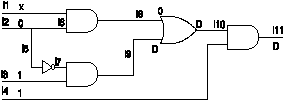
Figure 5. An illustrative example
Figure 6 shows the steps performed by the VHDL gate models and test bench for finding a test for l9 Sa0. Initially the test bench activates a D on l9. The OR and its following AND models propagate this value to the primary output of the circuit. After 1 femtosecond the output value is assigned back on itself to activate the gate model in the backward mode (Step 4 in Figure 6). Each model sensing an event on its output will justify its output value by assigning values to its inputs (Steps 5 to 10). When justification process reaches the primary inputs a test is found for the activated fault and is reported by the testbench.
1.	Activate D on l9.

2.	Propagate D to l10.

3.	Propagate D to l11.

4.	Wait for 1FS, assign D to l11.

5.	Justify D on l11 by assigning
	"D1" to lines l10 and l4 respectively.

6.	Justify D on  l10 by assigning
	"0D" to lines l8 and l9 respectively.

7.	Justify '0' on l8 by assigning "X0"
	to lines l1 and l6 respectively.

8.	Justify D on l9 by assigning "11"
	to lines l7 and l3 respectively.

9.	Justify '1' on l7 by assigning '0' to   l5.

10.	Justify '0' on l5 and l6 by assigning '0' to l2.

11.	Vector "X011" on l1 through l4 is a test
	for the desired fault.
|
Figure 6. Events in test generation for l9 Sa0 in Figure 5
4.2. What If Conflicts Occur?
In certain cases when justifying values, two conflicting values may reach a fanout node. In this case, the fanout node should inform the driving gates that a conflict exists and all gates must try to resolve this situation. In such cases, gates may be able to resolve the conflict locally, or they have to propagate the conflict to other gates they are driving. In this section we will discuss the situation that gates can resolve conflict locally. Figure 7 shows a conflict that occurs when the AND gate requires a '0' output and the OR gate requires a '1' output.
Before a conflict propagates out of the local area it has occurred, we will make sure that all gates in this local area have tried all their possibilities. For example for the conflict shown in Figure 7 the AND gate or the OR gate can resolve the conflict by choosing another set of input values that can still lead to the same output value of the gate. For this reason, before a gate propagates a conflict to its output, it insists on its values, so that other gates in this local conflict will consider resolving the situation.
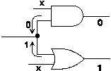
Figure 7. Illustration of a conflict
4.2.1. Gates That Do Not Insist On The Input Values
A conflict can simply be resolved if gates that have option in changing their input values inform the conflicting node of their possible input change. Consider the example shown in Figure 8. VHDL gate models for the generation of a test vector for l9 Sa0 (D) fault, behave as outlined in Figure 9.
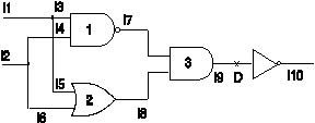
Figure 8. Local conflict resolution; non insisting
1.	Activate D on l9.

2.	Propagate D to l10.

3.	Wait for 1FS, assign DBAR to l10.

4.	Justify DBAR on l10 by reassigning
	D on l9.

5.	Justify D on  l9 by assigning  "11"
	on lines l7 and l8 respectively.

6.	Justify '1' on l7 by assigning "0X"
	on lines l3 and l4 respectively.

7.	Justify '1' on l8 by assigning "1X"
	on lines l5 and l6 respectively.

8.	Conflict occurs on fanout node l1.
|
Figure 9. Sequence of events in test generation for Fig. 8
Step 8 of Figure 9 indicates that a conflict on l1 has occurred because gates connected to that node are asking for inconsistent logic values. A resolution function at that node detects the conflict and informs all conflict causing gates of this situation. Depending on the number of '1's and '0's that participate in a conflict, the resolution function produces one of the following values:
CM0 : Conflict with Majority of driving values being '0'.
CM1 : Conflict with Majority of driving values being '1'.
If number of '1's and '0's in a conflict are the same, the resolution function arbitrarily chooses CM0 to report to the conflict causing gates. In our example, the resolution function at node l1 places CM0 on lines l3 and l5.
Placing CM0 or CM1 on the inputs of the gates makes gates to reconsider their driving input values. A gate having '0' ('1') driving value that finds a CM0 (CM1) value reported to it by the resolution function will not take any action. On the other hand, a gate having a '0' ('1') driving value that finds a CM1 (CM0) value reported to it by the resolution function will consider changing its input values to conform to the majority values from the resolution function. If the gate can make this change, it will report its new value to the resolution function, otherwise it will insist on its value by returning a IO0 (IO1) value to the resolution function.
The sequence of events that occur in the example of Figure 8 after those of Figure 9 are shown in Figure 10.
9.	Resolution function generates CM0.

10.	G1 takes no action.

11.	G2 changes its input values to "X1" on
	lines l5 and l6 respectively.

12.	Resolution function at node l1 finds all
	agreeing driving values and produces a '0'
	on that node.

13.	The conflict resolves, and so the desired
	test pattern is generated.
|
Figure 10. Events after occurrence of a conflict
In this example, G2 that finds itself being the cause of the conflict (according to the returned value from resolution function), and finds that it can still produce the output value '1' by selecting "X1" on its inputs, will simply choose this value set and report it to both inputs. The resolution function resolves '0' and 'X' to '0' and reports it to all lines connected to the node. Note that while this is happening, the resolution function on node l2 is also active in detecting and setting values. Initially this resolution function sees two 'X' values on lines l4 and l6 and returns no conflict. When the resolution function of node l1 resolves its conflict, the resolution function of node l2 sees an 'X' and a '1' on lines l4 and l6 which is still a non-conflicting value set. Finally, values '0' and '1' are generated on nodes l1 and l2 respectively.
If a gate can not change its input values, it returns insisting value to the resolution function. This situation will be discussed in the following section.
Figure 11. Local conflict; insisting on present values
4.2.2. Gates That Insist On Their Values
A different situation than that presented in the previous section is that the gate seeing a conflict on its input can not change its input value and therefore insists on its existing value. We will use the example of Figure 11 to illustrate this case.
For detecting a Sa0 on line l5, a D value is placed on this line. The sequence of events for propagation and justification of this value is shown in Figure 12. As shown in Step 6 of Figure 12, a normal propagation and justification causes a conflict on the fanout node of circuit of Figure 11. As in the previous section, the resolution function tries to resolve the conflict by placement of CM0 and CM1 on lines l3 and l4. Assuming a CM0 is placed on lines l3 and l4, G2 finds that it can not change its l3 input to agree with the presented majority (CM0) vote. It will therefore insists on its '1' value by assigning an IO1 to this line (IO0 and IO1 stand for Insist On '0' and Insist On '1' respectively).
1.	Place D on l5.

2.	Propagate D to l6.

3.	Wait for 1FS, Place D on l6.

4.	Justify D on output of G2 by assigning '1'
	to l3.

5.	Justify D on l5 by placing "0X" on l4
	and l2 respectively.

6.	Conflict occurs because two stems of
	a fanout (l3 and l4) have inconsistent values.
|
Figure 12. Events in test generation for Fig. 11
This value tells the resolution function to try to make the majority values agree with the minority values. The sequence of events after occurrence of the conflict at the fanout node that follow Step 6 of Figure 12, is shown in Figure 13.
7.	Resolution function generates CM0.

8.	G1 takes no action.

9.	G2 finds that it can not change its input
	from '1' to '0' and therefore generates IO1.

10.	Resolution function issues CM1 to make
	majority change according to the will
	of minority.

11.	G2 sees CM1 and takes no action.

12.	G1 sees CM1 and changes its inputs to "X0"
	on lines l4 and l2

13.	The conflict resolves.
|
Figure 13. Events after occurrence of a conflict
Following step 10 of Figure 13, G1 keeping the same output value, changes its two inputs from "0X" to "X0" causing the resolution of the conflict. At this point the final node value becomes '1' which agrees with all driving values.
4.3. What If Conflicts Grow Out Of A Local Area
In the previous section conflicts were resolved by either of gates that contributed to the creation of the conflict. In this section we will describe the case that a conflict can not be resolved locally. Consider the example of Figure 14. For a Sa1 on l6, the fanout node driving stems l2 and l3 has a '0' on l2 and a '1' on l3. According to the sequence of events of Figure 15, this conflict must be propagated beyond G1 into G2.
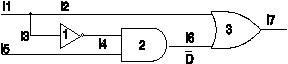 Figure 14. Conflict resolution; out of the local area
Events shown in Figure 15 indicate that a conflict grows out of a local area, and causes other values to change. The new values will be propagated back to the original conflict area when resolved.
Figure 14. Conflict resolution; out of the local area
Events shown in Figure 15 indicate that a conflict grows out of a local area, and causes other values to change. The new values will be propagated back to the original conflict area when resolved.
1.	Assign DBAR on l6.

2.	Propagate DBAR to l7.

3.	Wait for 1FS, assign DBAR to l7.

4.	Justify DBAR on l7 by assigning a '0' on l2.

5.	Justify DBAR on l6 by assigning "0X" on
	l4 and l5 respectively.

6.	Justify '0' on l4 by assigning a '1' on l3.

7.	Conflict occurs on the fanout node whose
	stems are l3 and l4.

8.	Resolution function produces CM0 to be
	considered by G3 and G1.

9.	G3 takes no action since it already has a '0'
	on l2.

10.	G1 produces IO1 on l3.

11.	The resolution function produces CM1 on l2
	and l3.

12.	G3 insists on its value by placing IO0 on l2.

13.	G1 places IO1 on l3.

14.	The resolution function produces CM0 to
	indicate that the majority can not agree with
	the minority vote.

15.	G1 again sees CM0 and knows that it can
	not force the majority to agree with it, so it
	changes its output from '0' to '1'.

16.	A '1' on l4 by G1 conflicts with '0' on l4
	by G2, and therefore the conflict is now
	beyond the local fanout node.

17.	Resolution function on l4 places CM0 on
	this line.

18.	G1 sees CM0 on its output and insists on
	this value by placing IO1 on this line.

19.	G2 takes no action.

20.	Resolution function produces CM1.

21.	G1 takes no action.

22.	G2 changes its inputs to "X0" on l4 and l5
	respectively.

23.	Conflict is resolved at l4.

24.	The Value '1' on l4 is justified by '0' on l3.

25.	Values on l3 and l2 agree, and the original
	conflict is now resolved.
|
3FONT SIZE=2 >Figure 15. Events in test generation for Figure 14
4.4. Reconvergent Fanout With Different Inversions
As in most test problems, test generation methods must give special attention to reconvergent fanouts. The situation becomes more difficult when fanout branches with different inversion parities converge. The main problem of reconvergent fanout is the possibility of propagation of fault via several paths. Using multiple paths to propagate a fault may result in one propagation path to be masked by another. On the other hand, choosing another set of fanout branches for fault propagation may properly lead the fault to occur on a primary output. We will therefore need a systematic exploration of the complete space of possible solutions in order to reach an appropriate set of propagating paths. In other words, for a fanout node with n branches, 2n-1 possible paths exist, only some of which may propagate a fault to a primary output.
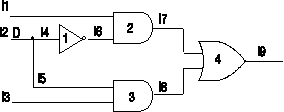
Figure 16. Illustration of reconvergent fanout problem
Our modeling strategy for this case is illustrated using the example shown in Figure 16. A Sa0 fault on l2 is propagated through both l4 and l5 paths, DBAR and D reach on l7 and l8 inputs of G4. These values ORed together cause a '1' on l9 which indicates that the error is not propagated to the output. Alternatively, we could try propagation of D value through various combinations of fanout branches and use the one that reaches the final output. For our case, propagation of D through only l4 branch would lead to a DBAR on the primary output.
In the VHDL implementation, in order to choose propagation branches and separate them from those that are not to propagate a fault, we use two new values NPD and NPDBAR (Non Propagating D or DBAR) to indicate that a fault is not to be propagated through a branch. Because different fanout branches take different values and also because the choice of the combination of values on fanout branches has to be remembered, we have used a fanout component at fanout nodes. Note that a resolution function, as is used in all other nodes, would not be capable of memorizing any information.
In the example of Figure 16, the fanout component at the fanout node would initially chose to propagate (D,D) on l4 and l5 from the set of { (D,D), (D,NPD), (NPD,D) } possibilities. As described above, (D,D) leads to a '1' on the primary output. The second choice (D,NPD) would cause the DBAR value to reach l9, while NPD at l5 remains on that line and the G3 gate does not react to this value.
4.5. Faults That Cannot Be Detected
Two Categories of faults can not be detected. One is undetectable and the other is aborted faults. The former occurs in circuits with reconvergent fanout(s). As described in the previous section a complete set of all possibilities of propagating through branches is tried at a fanout node. If all possibilities are tried, and none of them leads to propagation of the desired fault to a primary output, the fault is declared as undetectable. Such faults occur only in circuits with redundancy [3].
The second category, referred to as aborted faults, are those that our method finds them hard to detect, and therefore declares them as undetectable. In section 4.4 if backtracking is repeated more than a fixed limit, the fault is assumed undetectable.
ENTITY test_gate2 IS
  PORT (i1, i2, o : INOUT TestSig := ('U',FALSE));
END test_gate2;
ARCHITECTURE behavioral OF test_gate2 IS
BEGIN
  PROCESS
  BEGIN
    WAIT ON i1.sig'TRANSACTION,
                      i2.sig'TRANSACTION,
	      o.sig'TRANSACTION;
    IF (NOW = Initialization time)
      THEN Initialize all signals and variables;
    ELSIF (i1.sig'TRANSACTION'EVENT OR     	i2.sig'TRANSACTION'EVENT)
      THEN IF (NOW = Fault Propagation time)
        THEN Propagate fault to the gate's output
      ELSIF (Conflict is occurred on inputs)
        THEN Try to resolve conflict according to the
                    returned value from resolution function and
                    then set inputs accordingly.  If this operation
                    has already been done unsuccessfully,
                    propagate conflict to the gate output;
      END IF;
    ELSIF (NOW = Time to justify AND
                   o.sig'TRANSACTION)
      THEN IF (There is no conflict on the gate's output)
          THEN Assign appropriate values to the
                    undetermined inputs of gate according to the
                    output value and other previously determined
                    inputs;
      ELSIF (current driving value is '0' or '1')
        THEN Insist on it;
      ELSE Assign 'U' to the output;
      END IF;
    END IF;
  END PROCESS;
END behavioral;
|
Figure 17. Outline of a 2-input NAND gate
4.6. VHDL Style
We have presented modeling details for VHDL gate models for test generation. In this part we will present a partial VHDL code that shows the outline of the model for a 2-input gate.
As shown in Figure 17, a gate model consists of a PROCESS that always waits until a TRANSACTION appears on one of its inputs or output. After this TRANSACTION, according to mode of operation and value of the signal that activates the PROCESS, initialization, error propagation, line justification or attempt in conflict resolution will be done. Details of these operations were discussed in the previous sub-sections.
5. Use Environment
The previous sections described VHDL models for basic logical gates. This section presents an environment in which a circuit description using the gate models can be used for generation of test pattern for the circuit. Figure 18 shows a general outline of the VHDL code for a testbench.
ENTITY  ckt_tester IS END ckt_tester;
--
ARCHITECTURE testbench OF ckt_tester IS
  COMPONENT
    uut PORT (port1, port2,..., portn:INOUT TestSig);
  END COMPONENT;
  FOR c1:uut USE ENTITY WORK.cktn(structural);
  CONSTANT   no_of_nodes : INTEGER := n;
  TYPE nodes_vec
        IS ARRAY (0 TO no_of_nodes) OF TestSig;
  TYPE undctfary
        IS ARRAY (0 TO no_of_nodes) OF BOOLEAN;
  SIGNAL   n : nodes_vec;
BEGIN
  Component instantiation;
  PROCESS
    VARIABLE   faultlist;
	-- list of all faults that must be detected
  VARIABLE undetectedfaults;
	-- At the end of program run, this variable
	-- contains all undetected faults
  BEGIN
    WHILE (all faults in faultlist are not considered)
     LOOP Select an unconsidered fault;
               Apply the selected fault to the
               corresponding node;
      Wait For 1FS;
      Generate a transaction on primary output;
      Wait for 1 FS;
	-- At this time either a test is generated
	-- for the selected fault or the fault is
	-- undetected  (undetectable or hard to detect).
      IF (the fault is not detected)
      THEN
            Update undetectedfaults variable);
      ELSE
             Update faultlist according to the generated
             test pattern);
      Initialize circuit nodes and prepare it for test
      generation of the  next fault
    END LOOP;
  END PROCESS;
END testbench;
|
Figure 18. A general outline of testbench
In this code the component for which test is to be generated (UUT, Unit Under Test) is instantiated. A process runs concurrent with this instantiation that applies fault, and reports the generated test pattern.
The faulting process uses a constant fault list. In a While-Loop it looks up a fault from the table and applies it to the UUT by placing a D or DBAR on the corresponding line. After several delta times the effect of the fault reaches the primary outputs. 1 femtosecond later, same output values are assigned to the PO lines. This causes a transaction on the outputs, and enters gates of UUT in the justification mode.
After several delta times, either a test is generated, or the fault is declared as undetected. If fault is detected, fault list array is updated by removing the present fault and other faults known to be detected by the generated test. The process described here for generating test vector continues until there are no more faults in the fault list.
ENTITY pexam1  IS  PORT
      ( l1, l3, l5, l2, l4, l6, l7, l8, l9, l10 : INOUT TestSig);
END pexam1;

ARCHITECTURE structural OF pexam1  IS
  COMPONENT
      nand2 	PORT (i1,i2, o	 : INOUT TestSig);
  END COMPONENT;
  COMPONENT
      or2     	PORT (i1,i2, o	 : INOUT TestSig);
  END COMPONENT;
  COMPONENT
      and2   	PORT (i1,i2, o   : INOUT TestSig);
  END COMPONENT;
  COMPONENT
      inv     	PORT (i, o       : INOUT TestSig);
  END COMPONENT;
  COMPONENT
      fo2     	PORT (i1, o1, o2 : INOUT TestSig);
  END COMPONENT;
BEGIN
  cp1 : fo2    	PORT MAP (l1,l3,l5);
  cp2 : fo2    	PORT MAP (l2,l4,l6);
  c1  : nand2 	PORT MAP (l3,l4,l7);
  c2  : or2     PORT MAP (l5,l6,l8);
  c3  : and2   	PORT MAP (l7,l8,l9);
  c4  : inv     PORT MAP (l9,l10);
END structural;
|
Figure 19. VHDL code of structural description of Fig. 8
Figure 19 shows an example VHDL description instantiated in the testbench of Figure 18. This is the description of the circuit of Figure 8 in which a conflict occurs for finding Sa0 fault on l9. Tests generated for this circuit for l1 Sa0 and l9 Sa0 are shown in Figure 20. This figure shows circuit node values during each step of the test generation process. Initial node values are 'U'. At (4 femtoseconds + 7 delta), a conflict has caused CM1 values on l3 and l5. This conflict is resolved to '1' by the resolution function. Test generated for l9 Sa0 is on the circuit inputs at (4 femtoseconds + 10 delta). After a test is found all circuit nodes are forced to 'U' by placing SU values on the circuit nodes.
(  Test vector for detecting l1 Sa0 fault.
   Note: test also detects l9 Sa1 and l9 Sa1)
FS+d  l1  l3  l5  l2  l4  l6  l7  l8  l9 l10

0+0    U   U   U   U   U   U   U   U   U   U
0+1    D   U   U   U   U   U   U   U   U   U
0+2    D   D  NPD  U   U   U   U   U   U   U
0+3    D   D  NPD  U   U   U  DBAR U   U   U
0+5    D   D  NPD  U   U   U  DBAR U  DBAR U
0+6    D   D  NPD  U   U   U  DBAR U  DBAR D
1+4    D   D  NPD  U   U   U  DBAR 1  DBAR D
1+5    D   D  NPD  U   1   U  DBAR 1  DBAR D
1+6    D   D  NPD  U   1   1  DBAR 1  DBAR D
1+7    D   D  NPD  1   1   1  DBAR 1  DBAR D
2+1    U   U  NPD  1   1   1   U   1   U   U
2+2   SU  SU  SU  SU  SU  SU  SU  SU  SU   U
2+3    U   U   U   U   U   U   U   U   U   U

(*  Test vector for l9 Sa0 fault *)
FS+d  l1  l3  l5  l2  l4  l6  l7  l8  l9 l10

3+1    U   U   U   U   U   U   D   U   U   U
3+3    U   U   U   U   U   U   D   U   D   U
3+4    U   U   U   U   U   U   D   U   D  DBAR
4+4    U   U   U   U   U   U   D   1   D  DBAR
4+5    U   0   U   U   X   U   D   1   D  DBAR
4+6    U   0   1   U   X   X   D   1   D  DBAR
4+7    U  CM1 CM1  X   X   X   D   1   D  DBAR
4+8    U   1   1   X   0   X   D   1   D  DBAR
4+9    1   1   1   X   0   0   D   1   D  DBAR
4+10   1   1   1   0   0   0   D   1   D  DBAR
5+1    1   1   1   0   0   0   U   1   U   U
5+2   SU  SU  SU  SU  SU  SU  SU  SU  SU   U
5+3    U   U   U   U   U   U   U   U   U   U
|
Figure 20. Tests generated for the circuit of Figure 19
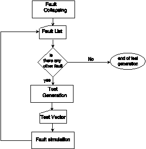
Figure 21 . A typical use environment
The above fault activation and test generation process is a simple example of many possible environments that can take advantage of test generation VHDL models. In a different environment, shown in Figure 21, a fault list can be generated by fault collapsing. The test generation will only generate test for each set of equivalent faults. A test generated as such is used in a fault simulator or a critical path tracing program for identifying all faults detected by the test vector, and removing them from the fault list. A testbench encompassing these components is possible in VHDL
6. Conclusions
We have used VHDL for test generation which is an important tool for design and analysis of digital systems. Although we have only considered combinational test generation, design for testability (DFT) techniques make such methodologies applicable to general digital circuits. In addition to test generation VHDL models, we have also developed VHDL models for fault collapsing, VHDL models for critical path tracing, as well as models for parallel fault simulation. After simulation and synthesis, test seems to be an appropriate area for using VHDL in digital system design automation.
Models presented here have been tested with most circuits available in various texts and literature. We have been able to generate test for all circuits found in literature that contain classical hard to detect faults.
REFERENCES
- [1] IEEE Standard VHDL Language Reference Manual, IEEE Std 1076_1987, The Institute of Electrical and Electronic Engineers, Inc., 1988.
- [2] Z. Navabi, VHDL: Analysis and Modeling of Digital Systems, McGraw_Hill Publishing, NewYork, NewYork, 1993.
- [3] M. Abramovici, M. A. Breuer, and A. D. Friedman, Digital Systems Testing and Testable design, New York, Computer Science Press, 1990.
- [4] V. D. Agrawal, K. Cheng, and P. Agrawal, " A Directed Search Method for Test Generation Using a Concurrent Simulator," IEEE Trans. on Computer-Aided Design, Vol. 8, No. 2, pp. 131-138, February, 1989.
- [5] F. E. Norrod, "An Automatic Test Generation Algorithm for Hardware Description Languages," Proc. 26th Design Automation Conf., pp. 429-434, June, 1989.
- [6] G. D. Robinson, "HITEST-Intelligent Test Generation," Proc. Intn"l.Test Conf., pp. 311-323, October, 1983.
- [7] T. J. Snethen, "Simulator-Oriented Fault Test Generator," Proc. 14th Design Automation Conf., pp. 88-93, June, 1977.